BLOG
ADDITIVE MANUFACTURED ANTENNAS AND RF COMPONENTS
March 2023

EFFICIENT PROTOTYPING & SMALL BATCH PRODUCTION
Additive manufacturing (AM), or 3D printing, has gained increased attention in recent decades. For several reasons, such as increased design freedom, reduced cost and production time, or increased manufacturing capability, AM has found its way into an engineer’s standard toolbox. AM has become a state-of-the-art fabrication technique, not only for rapid prototyping but also for low volume production.
Examples of AM manufactured structures.
During their triumphal march, AM technologies have evolved in many aspects. Today, there are different AM methods, such as filament deposition modeling (FDM), stereolithographic sintering (SLS), stereolithography (SLA) or material jetting (PolyJet™, MultiJet™), as well as different materials available. This includes not only several plastics but also 3D printing of conductive materials (metal).
In the first part of this article, we will provide a brief introduction to additive manufacturing processes. While this introduction does not claim to be complete, we provide a basic understanding of common printing methods, the resulting advantages and disadvantages and related design restrictions. Although AM is available for many different materials, such as plastic, metal, glass or ceramic, we focus on plastics, mainly for reasons of cost effectiveness and weight.
In the second part, we discuss AM for RF components and antennas. This section focusses on structures, printed from dielectric materials, followed by conductive coating (metallization). This choice is again motivated by cost and weight considerations.
Please note that by RF components, we understand structures interacting with an electromagnetic field in a certain desired way. These elements are not small compared to the wavelength, opposed to lumped components, such as ideal Resistors, Capacitors or Inductors. In this sense, RF components include components such as antennas, waveguides, cavity resonators and others.
ADDITIVE MANUFACTURING METHODS
FDM
Filament Deposition Modeling
One of the most popular AM methods is FDM, also known as fused filament fabrication (FFF).In this process, a thermoplastic material is pushed through a hot nozzle to deposit dielectric material (extrusion). By moving the nozzle during this deposition process, the part builds up in layers of strings or ropes of the dielectric material. The base material is continuously provided as filament from a spool. This simple but effective setup makes FDM a very cost efficient and popular 3D printing method.
For FDM, a 3D part needs to be translated into movement of the nozzle for printing. For this, the part is usually sliced into layers in height or z-direction. For each layer, the nozzle movement within the xy-plane determines how the material deposit builds up the part. This job is typically performed by a piece of software, referred to as the slicer. As illustrative example, we provide a figure of a cuboid with an internal spherical cavity below.
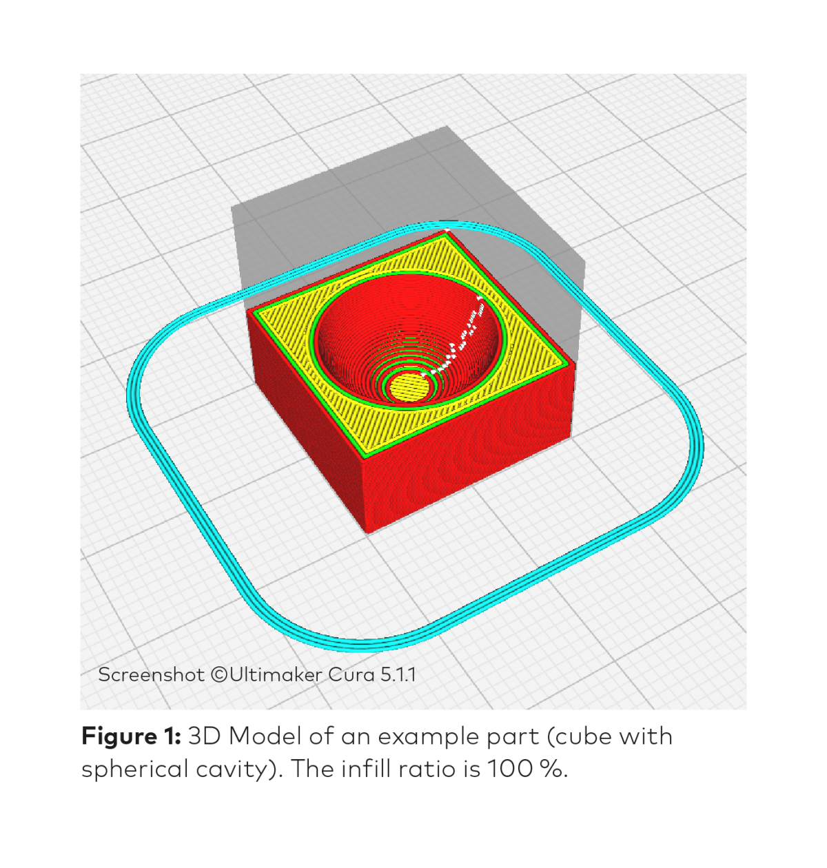
Figure 1 clearly shows how the layers are formed by relative nozzle movement and how the layers add up to the complete part. Material deposition on the part’s outside is indicated in red. This is also called “outer layer”. The second outer layer is indicated in green and material deposition on inner layers is shown in yellow for visual guidance.
The understanding of how parts are 3D printed by FDM also reveals the method’s limitations. The width and height of the string-like material deposit is subject to the printing system and mainly depends on the nozzle and print speed. This leads to a certain granularity or resolution of the 3D printed part.
The understanding of how parts are 3D printed by FDM also reveals the method’s limitations. The width and height of the string-like material deposit is subject to the printing system and mainly depends on the nozzle and print speed. This leads to a certain granularity or resolution of the 3D printed part.
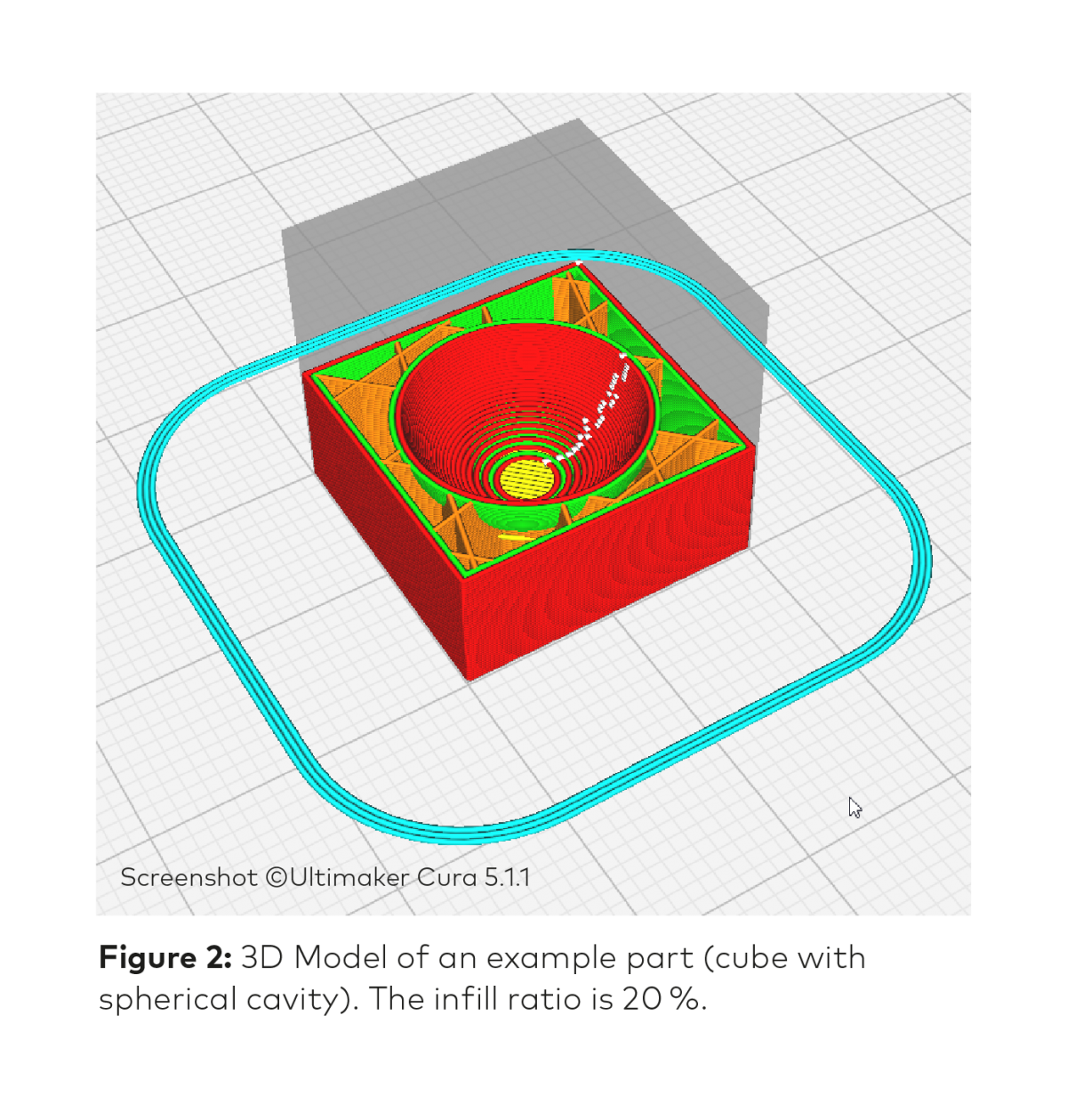
Another distinct feature of AM compared to traditional fabrication processes is infill. Although this concept is not unique to FDM, we explain it in this context. Infill describes how a given volume is filled with the print material. The ratio of volume filled with the printed material to the total volume is known as infill ratio. The smallest volume for which this consideration holds, is referred to as the unit cell. Spatial repetitions of this cell make up the core of a part with infill ratio smaller than one. To illustrate this concept, we provide Figure 2, showing the same example part as before. In this case, the infill ratio was set to 20 % with a “tri-hexagon” infill pattern.
SLS
- Stereolithographic Sintering
The AM method SLS employs a high-power laser source to generate heat, required for the sintering process. The base material, which might be plastics but could also be metal or glass, is provided as a thin layer of powder. The fine particles are then melted by a pulsed high-power laser source, which is scanned across the layer. After this step, another layer of material is added to the powder bed. This way, like FDM, the 3D structure is built up layer by layer. The AM process itself is more complicated to handle compared to FDM, since a laser is involved, and the base material is a fine powder rather than a simple solid filament.One of the main differences compared to FDM is the fact that the printed structure is fully embedded in the base material powder during the AM process. This allows manufacturing of parts with overhanging geometries without the need for supporting structures. Since the base material is provided as very fine powder, the process resolution is much finer compared to FDM.
On the other hand, printed structures can never be hollow and fully closed, since the non-melted powder could not be removed in this case. Therefore, internal empty cavities cannot be manufactured using SLS. Our previous example of a spherical cavity inside a cube could not be printed using SLS without further modification.
SLA
- Stereolithography
In SLA, a solid structure is generated by solidifying a liquid resin using a laser. Other than in SLS, where a laser is used to generate heat, in SLA a UV laser induces a photochemical reaction to cure the photopolymer resin.In most SLA processes, the laser is placed underneath a container with an UV transmissive bottom, which is filled with the resin. A moveable platform or baseplate in the container is illuminated by the laser, leading to a buildup of solid material at the bottom of the platform. After laser curing a layer of the structure to print, the platform is moved up and the next layer is cured by the laser. In this process, the printed part is sequentially pulled out of the liquid resin in the +z-axis direction against gravity. Due to this configuration, parts way bigger than the container can be printed.
Although this AM method is known to provide very good manufacturing performance in terms of surface finish, resolution and accuracy, the process is quite elaborate. Handling of liquid chemicals and a UV laser is required. Further, the printed parts must be cleaned with a solvent to remove residual resin. Since the base material is liquid, supporting structures are required for overhanging geometries. Like SLS, manufacturing parts with fully closed cavities are not possible since the resin would be trapped inside.
Material Jetting
To overcome these processing issues and increase design flexibility, other (proprietary) AM processes were developed. Material jetting deposits resin from a printing head equipped with many tiny nozzles, like classical inkjet printing on paper. The resin is UV cured immediately after deposition, generating a solid layer. This way, a part is again built-up layer by layer. Since only the required amount of resin is deposited and all the resin is UV cured, there is no need for cleaning with resin solvent after printing. Further, since this method does not build up parts in containers filled with powder or liquid, fully closed empty (air filled) cavities can be manufactured.
This concept is taken even one step further to arrive at so called additively manufactured electronics (AME). By combining conducting and isolating materials in the same 3D printing process, structures including internal electrical connections can be printed, where electronic components may be placed
on the surface. AME offers an alternative to classical PCBs, which are limited to planar designs, since the AM process offers 3D structures.
RF COMPONENTS
When it comes to AM of RF components or antennas, the potential for gaining advantage of the novel manufacturing process is manifold. Not surprisingly, however, 3D printing of RF components has many challenges on its own.
A first logical step from custom engineered RF parts such as waveguides or resonators could be AM with conductive materials, that is, 3D printed metals. This step already exploits advantages compared to conventional manufacturing processes such as milling and/or turning, which is production time, design freedom and prototype cost. Production time is especially of interest in a rapid prototyping context within research and development. Design freedom refers to the fact that structures like internal (rectangular) holes or cavities are straight forward to print while they are troublesome in conventional machining.
In an RF context, this is especially interesting in terms of waveguide components or cavity resonators. Avoiding milling or even more complex traditional manufacturing methods such as broaching or electric discharge machining leads to significant reduction in production cost and time.
While the step from traditionally manufactured metal parts to AM conducting parts is logical, the famous skin effect allows to take the evolution of RF component manufacturing one step further. The skin effect describes that the current density of alternating current is largest at the surface of the conductor. The amplitude of fields within a conductor decay to 1/e or 36.8%, after the distance

Skin Effect Formula
known as skin depth δs [1] with angular frequency ω, permeability μ and conductivity σ. In the field of RF engineering, the frequency of the alternating current is high, and the skin depth is therefore very small. For example, the skin depth in pure copper at a frequency of 1GHz is only 2.06μm. Therefore, RF fields do not penetrate conductors and only the outer appearance of a conductive structure is relevant when considering distributed RF components.
This leads to the second evolution of AM of RF components which is 3D printing of dielectric materials, followed by coating with a conductive material, that is, metallization.
Once the outer surface of a structure is coated uninterruptedly with a well conducting material, the core structure is free of electromagnetic fields and therefore does not play any role for the functionality of the 3D printed RF component. Metallization of 3D printed materials thereby almost entirely decouples the choice of AM technology and dielectric material independent of the RF component’s function, given the dielectric material is suitable for the metallization process.
The major advantage of metallized dielectric 3D printed RF components and antennas is weight. Dielectric materials generally offer much lower mass density compared to metals, even when considering light metals such as aluminum, titanium or magnesium. Additionally, AM offers the ability to form internal cavities and infill ratios way below 100%.
This means that the 3D printed part is not only made from a low mass density material but is not even solid inside. The potential weight saving is therefore huge. Since the metallization layer is very thin, the weight of the metal coating on a 3D printed RF component is small. An RF device, such as an antenna, a waveguide, or a cavity resonator, produced through AM and metallization will weigh only a fraction compared to the same part made from solid metal. If the 3D printed part is, however, coated with highly conductive material such as copper, gold or silver, the part’s RF performance is virtually the same as if the component was solid metal. The high conductivity of the coating ensures that there is no electromagnetic field penetrating the coating according to the skin effect. The lightweight aspect makes AM of antennas and other RF components especially interesting for aerospace applications.
Drawbacks
There are, of course, also drawbacks and challenges related to AM. In terms of the described RF applications, they are mostly related to the metallization and surface finish. As already discussed, in the RF domain, electrical currents will only be present at the surface of a conductor. This leads to the logical conclusion that surface finish matters! Surface roughness is a critical parameter for losses in high frequency applications. Many RF components, such as large inductors, waveguides or horn antennas are therefore made from brass, followed by silver plating and polishing. The combination
of silver, the metal with highest conductivity, and a smooth surface, lead to low losses in practical implementation of RF parts. For the described process of 3D printing RF parts, the surface roughness is determined by the AM method as well as the metallization process.
of silver, the metal with highest conductivity, and a smooth surface, lead to low losses in practical implementation of RF parts. For the described process of 3D printing RF parts, the surface roughness is determined by the AM method as well as the metallization process.
METALLIZATION
As explained above, the conductive surface is the most important aspect of a distributed RF part. The 3D printed part’s large-scale surface finish is determined by the AM method. This surface roughness’ scale might be quite large and lies in the order of many micrometers. Still, a thin conductive coating
of a few micrometers thickness on such 3D printed part leads to good RF performance in terms of surface conductivity.
Plating with a highly conductive layer may be done through electroplating. Just like AM, this process is economically attractive. Electroplating, however, requires a conductive part to begin with. As mentioned before, a brass part, for example, would be silver plated through electroplating for increased surface conductivity in an RF application. When the structure to be plated is dielectric, a first conductive layer must be applied in a non-galvanic process. A common choice for this step is an initial coating with conductive paint, applied via spray painting. After this step, the surface of the printed part is sufficiently conductive to enable classical electroplating.
A typical metallization layer stack-up includes copper as initial layer due to its high conductivity, enabling electroplating with other metal layers, such as silver.
Often gold is the desired finishing outer metal layer due to its good conductivity and chemical stability. This, however, requires an additional nickel (or silver) layer in between the copper layer and the gold layer to prevent migration of gold into copper. This layer stack-up is widely used in PCB manufacturing, known as Electroless Nickel Immersion Gold (ENIG).
While this process is not desirable in RF applications due to the high losses introduced through the ferromagnetic nickel layer, this stack-up is not problematic for metallization of 3D printed dielectric parts. As explained before, only the outer conducting layer is relevant if the frequency is sufficiently
high, since the electromagnetic field concentrates within the first few micrometers due to the skin effect.
The Alternative
An alternative to the rather elaborate metallization process of spray painting and electroplating might evolve through recent advances in conductive filament materials. By employing a dualextruder 3D printer, the core of a part could be printed with a classical dielectric material while a conductive material could be used on the outer layer(s). Current conductive materials for FDM 3D print are, however, not sufficiently conductive to achieve acceptable surface conductivity for RF applications to the best of the authors knowledge.
Non-Metalized RF Components
Another application of AM is the fabrication of dielectric lenses. Lenses are used to improve directivity of the antenna. To achieve that, it is necessary to convert a spherical wave into a plane wave to achieve bundling. If the wavelength is small compared to the physical dimension of the lens, the function is very similar to optical lenses.
We distinguish between classical lenses and integrated lenses. A classical lens design has the focal point outside the structure and the refraction is performed on the surface of the lens, see Figure 4.
We distinguish between classical lenses and integrated lenses. A classical lens design has the focal point outside the structure and the refraction is performed on the surface of the lens, see Figure 4.
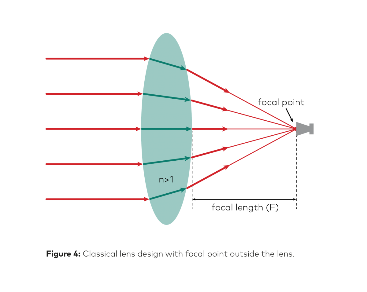
Unfortunately, this design requires a distance equivalent to the focal length of the lens between the source (waveguide) and the lens, yielding a space-inefficient design. Alternatively, an integrated lens is designed such that the focal point lies at the surface of the lens, see Figure 5.
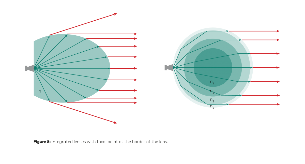
Integrated lenses with focal point at the border of the lens.
Integrated lenses either have a homogeneous or non-homogeneous refractive index. In both cases, the design including the feed (waveguide) is much more compact compared to the classical lens design.
For non-homogeneous lenses, variation of the infill ratio below 100% is used to achieve different refractive indices throughout the lens structure. Hereby a high infill ratio results in a higher effective permittivity while a lower infill will lead to a lower effective permittivity.
In practice, the infill pattern type itself can influence the resulting infill ratio due to printer accuracy. FDM test prints show that not only the realized infill ratio differs from what was set in the slicer, but this deviation also depends on the chosen infill pattern [2]. Furthermore, isotropy needs to be considered for design and manufacturing. Structured patterns, like a honeycomb pattern, lead to non-isotropic behaviour while a random pattern, which has no preferred direction, will lead to isotropic behaviour. AM provides a cost-efficient way to produce the desired dielectric properties by selecting a suitable infill pattern. This AM specific additional design freedom allows further reduction of lens size and weight compared to classical manufacturing methods.
SUMMARY
AM has become a state-of-the-art manufacturing method, not only for rapid prototyping but also for small volume series production. Today, there are many different 3D printing processes available, offering various possibilities and benefits for an engineer’s design process.
When dielectric structures are coated with highly conductive material, they behave as if there were made from solid conductors in the RF domain. This allows 3D printing of antennas and other RF components, which offer a significant reduction in weight and fabrication cost compared to classical manufacturing.
Even when considering plastics without metallization, AM offers benefits to the RF designer. The concept of infill allows to internally vary the density of a printed part. Therefore, lens antennas with varying dielectric constants can be printed. These designs are very tedious or even impossible to manufacture in a classical process and offer reduced weight, size and cost.
References
[1] D. M. Pozar, Microwave engineering, 4th ed. Hoboken, NJ: Wiley, 2012.
[2] J. Huang, S. J. Chen, Z. Xue, W. Withayachumnankul, and C. Fumeaux, “Impact of Infill Pattern on 3D Printed
Dielectric Resonator Antennas,” in 2018 IEEE Asia-Pacific Conference on Antennas and Propagation (APCAP),
Auckland, Aug. 2018, pp. 233–235. doi: 10.1109/APCAP.2018.8538296.
[2] J. Huang, S. J. Chen, Z. Xue, W. Withayachumnankul, and C. Fumeaux, “Impact of Infill Pattern on 3D Printed
Dielectric Resonator Antennas,” in 2018 IEEE Asia-Pacific Conference on Antennas and Propagation (APCAP),
Auckland, Aug. 2018, pp. 233–235. doi: 10.1109/APCAP.2018.8538296.
To download this blog article as a PDF, please log in here . Or register using the form below.
Would you like to be able to download all blog posts as PDFs and see all case studies in the full version?
Join the PIDSO insights section and see all case studies in the full version and get insights into our technical approach to this challenge.
